
Design for Testability (DFT): Adding pogo-pin pads the right way
How to layout your PCB so the factory can build a reliable bed-of-nails test jig without driving up manufacturing costs.
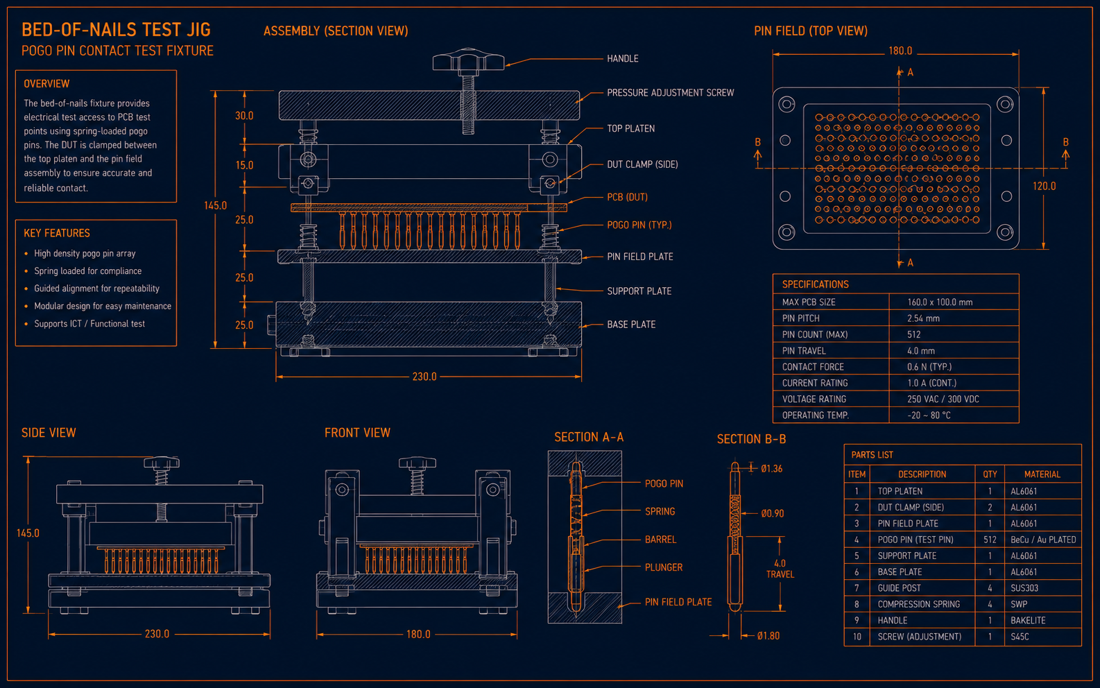
Design for Testability: adding pogo-pin pads the right way
A bed-of-nails test jig is only as good as the pad layout it's testing against, and pad layout is a decision made by the PCB designer — often long before anyone talks to the person building the test fixture. Getting this handoff right avoids an expensive redesign of either the board or the fixture.
Pad size and spacing aren't arbitrary
Standard pogo pins come in common tip diameters (0.68 mm, 1.02 mm, 1.52 mm being typical families), and your test pad needs to be sized to reliably capture the pin tip with some misalignment tolerance — not sized to the theoretical minimum. Spacing between adjacent test pads needs to account for the physical diameter of the pogo pin barrel, not just the tip, or neighboring pins will physically interfere with each other on the fixture.
Keep test pads off the component side when possible
Placing test pads on the bottom side, opposite populated components, means the bed-of-nails fixture can press directly without needing to route around tall components — this alone often determines whether a single-sided fixture is possible or whether you need a more expensive clamshell design.
What actually needs a test point
Not every net needs a dedicated pad. Prioritize:
- Every power rail, at multiple points if the rail is long, to catch resistive drops or opens
- Every microcontroller reset, boot-mode, and programming/debug interface line
- Key digital I/O and communication bus signals (SPI, I2C, UART) that functional test needs to exercise
- Ground reference points distributed near the signal test points, not just one global ground pad — a single distant ground reference adds measurement error on high-speed signals
Keep-out zones the fixture builder will thank you for
Leave a keep-out area around each test pad clear of tall components and connectors so the pogo pin has a clean, perpendicular approach — pins that have to compress at an angle wear out faster and make less reliable contact, and this is a common source of a fixture that "works most of the time."
The cost trade-off nobody skips
Every test pad added to the PCB has a real cost: board area, and often an extra layer or two if you're routing dense high-speed nets around required test access. The right number of test points comes from a conversation between the electrical designer and whoever owns test coverage requirements early in layout — not a wish list added after the board is finalized, when adding pads means a respin.
Takeaway: DFT succeeds or fails based on decisions made during PCB layout, not at the fixture-design stage — get the test engineer and PCB designer talking before layout is locked, not after.