
PCB design for motor control boards: 7 mistakes we keep seeing
Large current loops, ground planes split in the wrong place, decoupling caps parked too far from the IC pins — small layout mistakes that make a big impact.
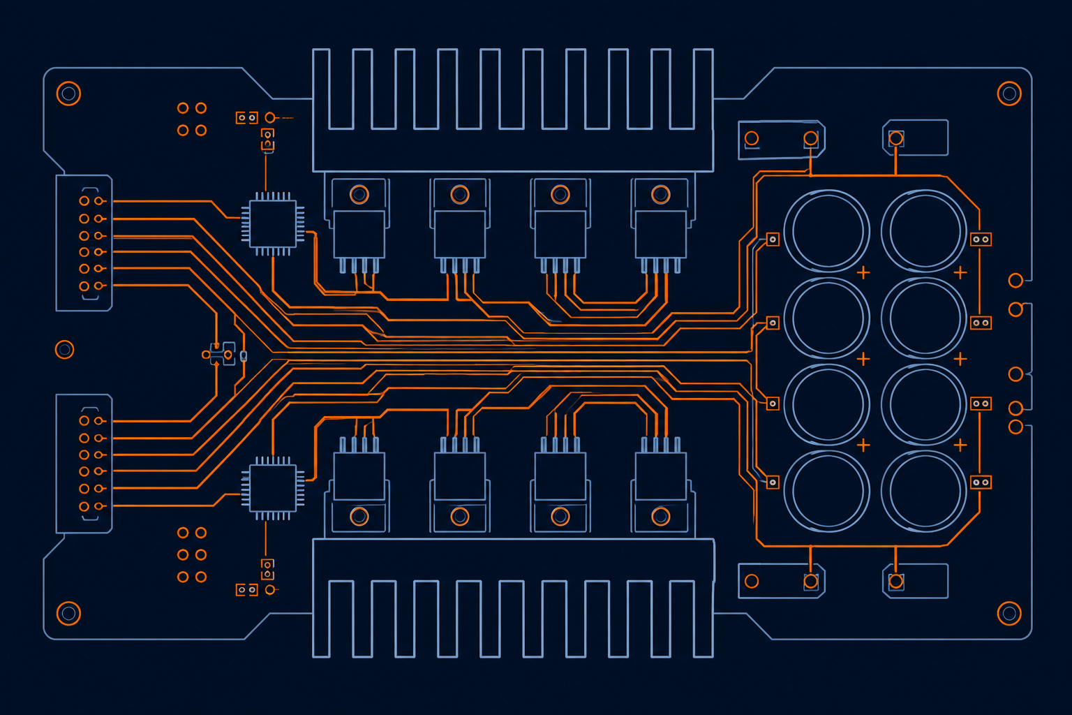
Why motor control boards fail in the field, not on the bench
Motor control PCBs rarely fail during bring-up. They fail three weeks into deployment, when the enclosure has heated up, the cable run to the motor is longer than the prototype's, and the load is drawing peak current instead of the nominal figure from the datasheet. Almost every field failure we've traced back traces back to one of these seven layout habits.
1. Current loops that are bigger than they need to be
The gate-driver-to-MOSFET-to-shunt loop is the single highest di/dt path on the board. Every millimeter of extra trace length adds parasitic inductance, and that inductance shows up as ringing on the switch node and as EMI you'll be chasing during certification. Keep the driver, the FET, the bulk capacitor, and the shunt resistor in one tight cluster — draw the loop first, then place everything else around it.
2. Splitting the ground plane in the wrong place
A single unbroken ground plane under the power stage is almost always the right answer. Teams split it to "isolate noise" and instead create a slot antenna, forcing return current to snake around the gap and radiate on the way. If you must separate analog and power grounds, join them at exactly one point, close to the ADC reference.
3. Decoupling capacitors placed too far from the pins
A 100 nF cap 8 mm from the IC's VDD pin might as well not be there at 20 MHz. Place decoupling directly against the pin, with the via straight down to the plane — not routed sideways first.
4. Undersized copper for continuous current
1 oz copper heats up fast under continuous motor current. Either move to 2 oz copper on the power layers or add copper pours with stitching vias to spread heat into inner layers.
5. Gate drive traces routed next to sensitive signal lines
High dv/dt gate traces coupling into an encoder or current-sense line will corrupt your control loop intermittently — the kind of bug that only shows up under load and is miserable to diagnose. Route gate drive on an inner layer, shielded by ground planes above and below.
6. No dedicated Kelvin connection for current sensing
Measuring shunt voltage from the same pad the power trace connects to picks up trace resistance and drops. Route separate Kelvin sense traces straight from the shunt pads to the amplifier input.
7. Ignoring thermal vias under the power stage
A MOSFET's thermal pad is only useful if heat has somewhere to go. Populate an array of vias under the pad connecting to a ground/heat plane, and consider an exposed copper area on the bottom side for a heatsink or enclosure contact.
Takeaway: none of these fixes are expensive — they cost design time, not BOM cost. Catching them at layout review is far cheaper than catching them during EMC testing or, worse, in a field return.